Steven Gives Invited Talk at the IOP Quantum Meets Nanoscale Workshop 2025
 Steven Schofield
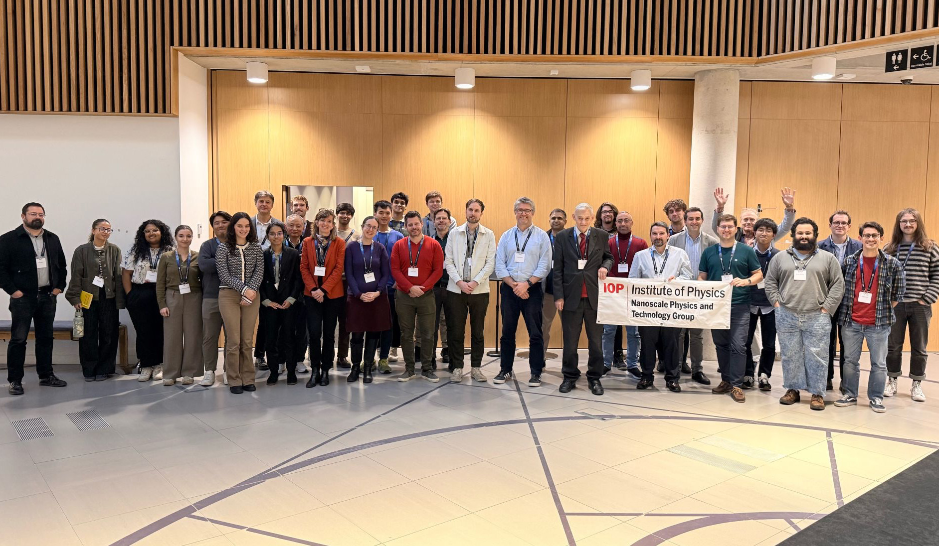
On Monday the whole group — Georgia, Sean, Byron, and I — attended the Quantum Meets Nanoscale Workshop (QMNW 2025), organised by the Institute of Physics Nanoscale Physics and Technology Group. The meeting brought together researchers working across quantum technologies, nanoscale materials, and advanced characterisation techniques, with a programme designed to highlight the many ways that nanoscience enables quantum technology, and how the drive to build new quantum devices is in turn stimulating new directions in nanoscience.
I gave an invited talk titled “Imaging and Understanding Quantum States in Semiconductors and 2D Materials” (slides available here), discussing how our group uses STM, SX-ARPES, and defect engineering to visualise and manipulate quantum states at the atomic scale. It was a pleasure to present this work in such an interdisciplinary setting, and to see a variety of ways in which nanoscience provides access to the investigation of fundamentally quantum phenomena.
James Millen (King’s College London) opened the scientific programme with a fascinating overview of optical levitation experiments on silicon nanorods and other nanoscale particles. His group uses tailored light fields to control both the translational and rotational motion of levitated objects, enabling exquisitely sensitive force measurements and offering routes toward creating macroscopic quantum superposition states. The characteristic revival dynamics associated with angular-momentum quantisation were a particular focus of his talk, illustrating how far beyond the atomic regime quantum control is now being pushed.
Rachael Oliver (University of Cambridge) followed with a wide-ranging tour of porous nitride semiconductors for quantum photonics. She discussed how GaN- and InN-based structures can be engineered to produce robust single-photon emitters, supported by detailed TEM imaging of dislocations and etched defect structures. This included some particularly striking TEM images of dislocation cores, showing the associated Burgers vectors directly – the kind of figure that would have been perfect for illustrating crystallography concepts in the PHAS0006 Thermal Physics and the Properties of Matter module I used to teach at UCL. Her talk emphasised that these materials, that are central to the LED industry, also offer rich possibilities for integrated quantum light sources, especially when crystal orientation and porosity are carefully controlled.
Matthew Cole (University of Bath) presented the challenges of developing field-emission devices from carbon nanotubes, and also from graphene sheets engineered to fold sharply at the nanoscale to act as high-performance emitters. While many simple CNT films underperform or degrade rapidly, his group uses CVD-grown CNTs and templated graphene structures to achieve stable emission with impressively high current densities. He showed how carefully controlled nanoscale morphology is crucial both to enhancing local electric fields and to preventing catastrophic avalanche burn-out.
Sandrine Heutz (Imperial College London) then explored how molecular semiconductors, particularly metal phthalocyanines, can be used to probe spin physics relevant to quantum technologies. By combining magnetic resonance with X-ray diffraction, her group maps hyperfine interactions with impressive clarity, revealing how molecular orientation influences spin behaviour. It was striking to see techniques from the OLED and photovoltaic also have application as tools for quantum science, including potentially quantum computing.
Kieran Orr (University of Cambridge), winner of the NPTG Thesis Prize, followed with an excellent overview of three-dimensional strain mapping in halide perovskites using Bragg coherent diffraction imaging and ptychography. His work links nanoscale strain and defect migration directly to photoluminescence variations, providing a compelling microscopic picture of how local structure influences optoelectronic performance.
The final invited talk of the day was given by Richard Forbes (University of Surrey), who presented his perspective on high electric fields in quantum systems and the broader implications for field-emission theory. The talk raised several points about inconsistencies and open questions in established quantitative models, offering a personal and thought-provoking viewpoint on an area with a long and complex history.
There were also several very strong contributed student talks. Thisarani Gnanarathne (UCL) discussed advances in quantum-dot–sensitised solar cells, Isabel Webb (UCL) presented progress toward metrological charge pumping for the new SI ampere, and Murad Alabdullah (Swansea University) spoke on quantum effects in nanoscale transistor simulations using 3D ensemble Monte Carlo methods. Together these talks added real breadth to the programme and highlighted the impressive work being carried out across the UK.
QMNW 2025 was an engaging and enjoyable meeting, with a programme that brought together a wide range of perspectives on the quantum–nanoscale interface. I’m grateful to the organisers for the invitation and for putting together such a thoughtful programme. This was the first meeting of its kind organised by the NPT group, and I hope they follow through on their intention to establish it as a regular fixture.