Publications
The group’s research spans both fundamental and applied aspects of nanoscience and quantum materials. Below is our full list of publications, with links to journal articles and preprints where available.
Use the search box to filter the publications list below
2025

Future of condensed matter physics for the next 10 years*
Journal of Physics: Condensed Matter
·
20 Oct 2025
·
doi:10.1088/1361-648X/ae0be1
Roadmap on atomically-engineered quantum platforms
Nano Futures
·
30 Sep 2025
·
doi:10.1088/2399-1984/ADE6B7
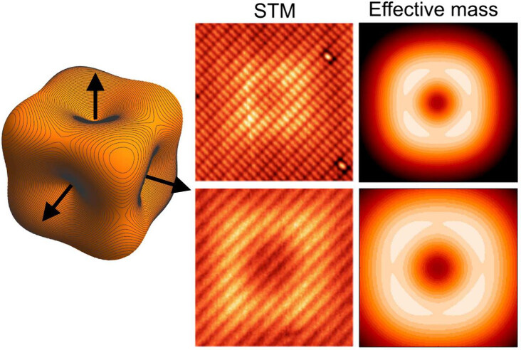
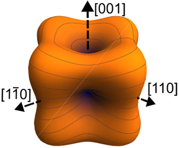
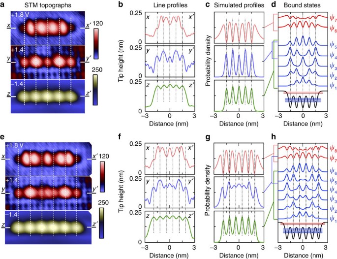
Imaging the Acceptor Wave Function Anisotropy in Silicon
Nano Letters
·
21 Aug 2025
·
doi:10.1021/acs.nanolett.5c02675
This paper presents the first STM imaging and spectroscopy of hydrogenic acceptor wave functions in silicon, with effective-mass and tight-binding theory confirming their square-ring-like symmetry and acceptor character.
Roadmap on atomic-scale semiconductor devices
Nano Futures
·
31 Mar 2025
·
doi:10.1088/2399-1984/ada901
This roadmap reviews 25 years of progress since Kane’s proposal for donor-based qubits in silicon, charting advances, challenges, and future directions in atomic-scale semiconductor quantum technologies.
2024
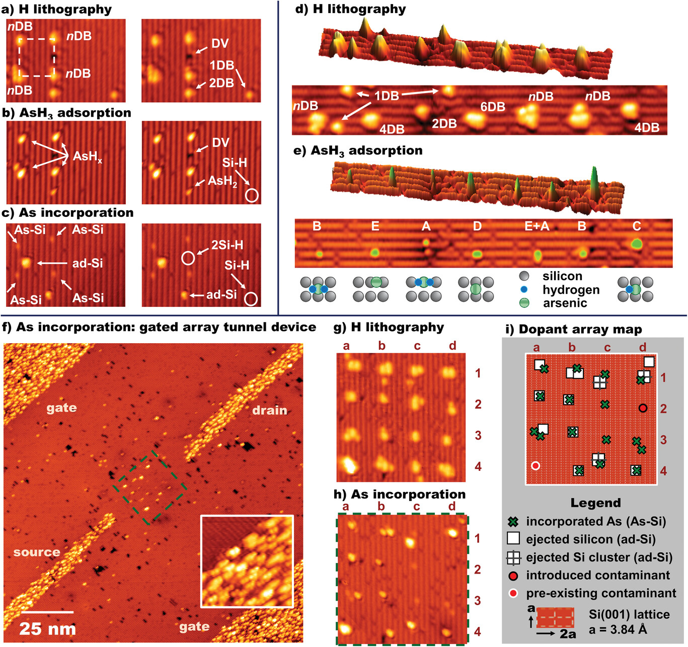
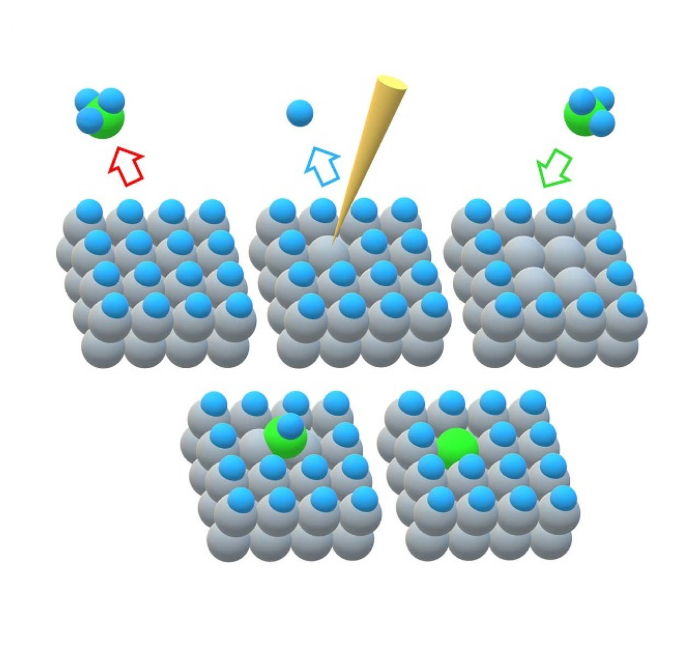
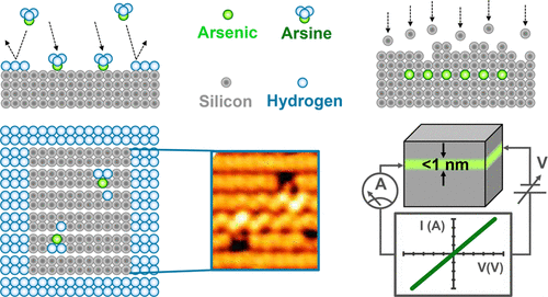
Single‐Atom Control of Arsenic Incorporation in Silicon for High‐Yield Artificial Lattice Fabrication
Advanced Materials
·
22 Mar 2024
·
doi:10.1002/ADMA.202312282
This work demonstrates deterministic placement of single arsenic dopants in silicon with 97 ± 2% yield, advancing the scalable assembly of atomically precise quantum devices.
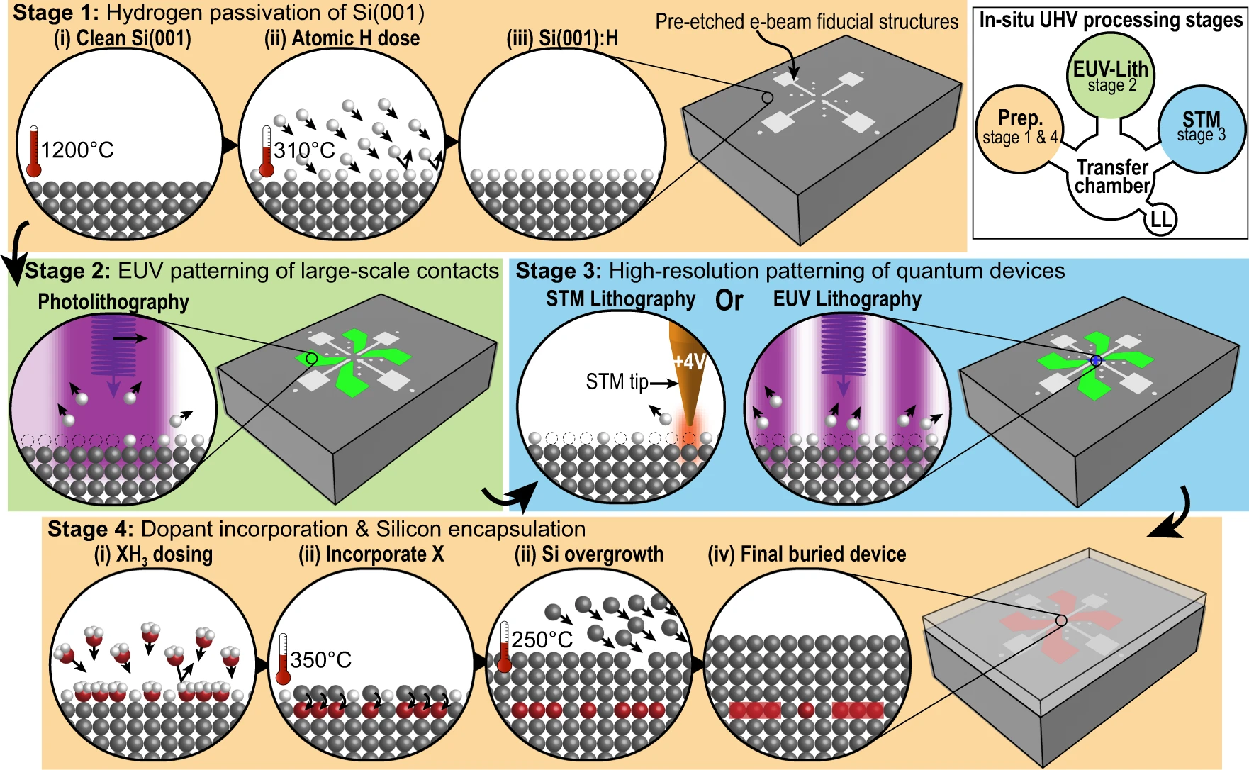
EUV-induced hydrogen desorption as a step towards large-scale silicon quantum device patterning
Nature Communications
·
24 Jan 2024
·
doi:10.1038/S41467-024-44790-6
This work demonstrates resist-free EUV-induced hydrogen desorption on Si(001):H, bridging atomic-precision STM lithography with scalable semiconductor manufacturing techniques.
2023
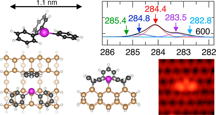
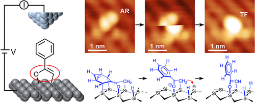
Adsorption and Thermal Decomposition of Triphenyl Bismuth on Silicon (001)
The Journal of Physical Chemistry C
·
14 Aug 2023
·
doi:10.1021/ACS.JPCC.3C03916
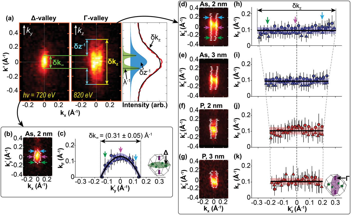
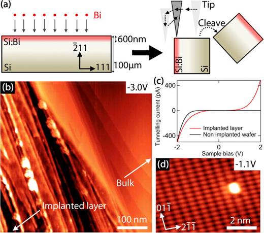
Momentum‐Space Imaging of Ultra‐Thin Electron Liquids in δ‐Doped Silicon
Advanced Science
·
19 Jul 2023
·
doi:10.1002/ADVS.202302101
This study demonstrates, for the first time, a non-destructive method to probe two-dimensional electron liquids in silicon, revealing their properties—including quantum confinement thickness—and showcasing the thinnest technological electron liquid to date (0.45 nm).
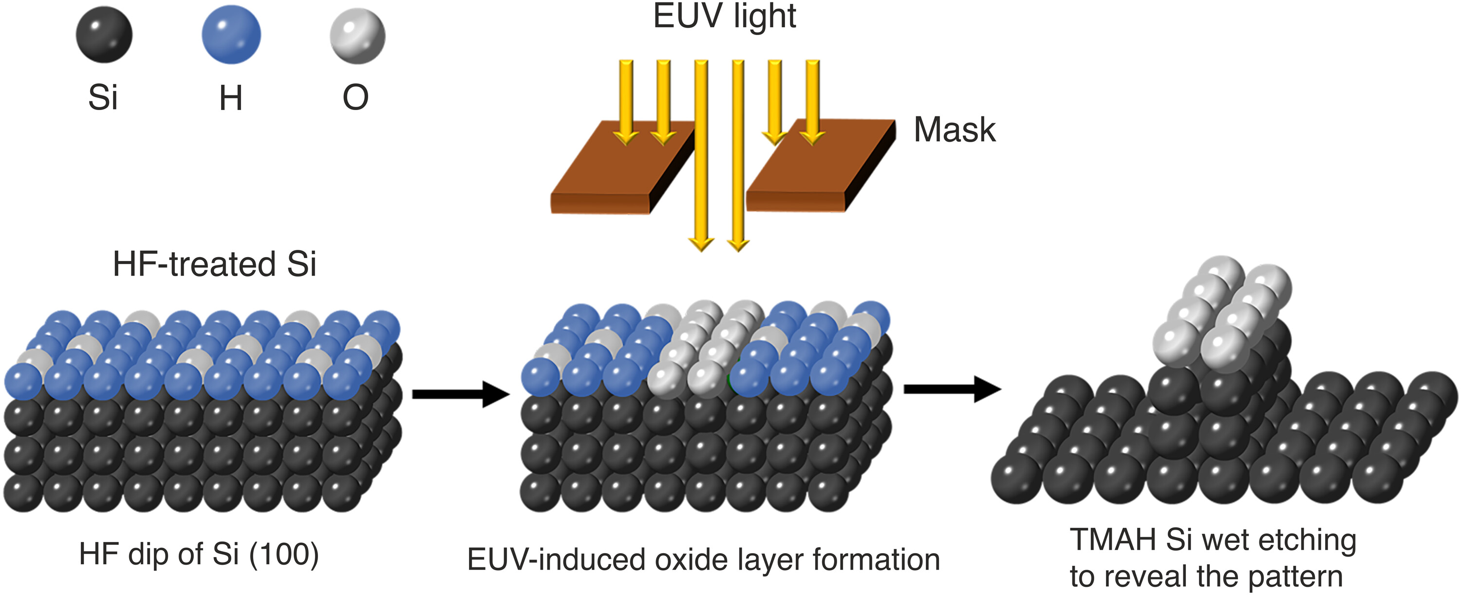
Resistless EUV lithography: Photon-induced oxide patterning on silicon
Science Advances
·
21 Apr 2023
·
doi:10.1126/SCIADV.ADF5997
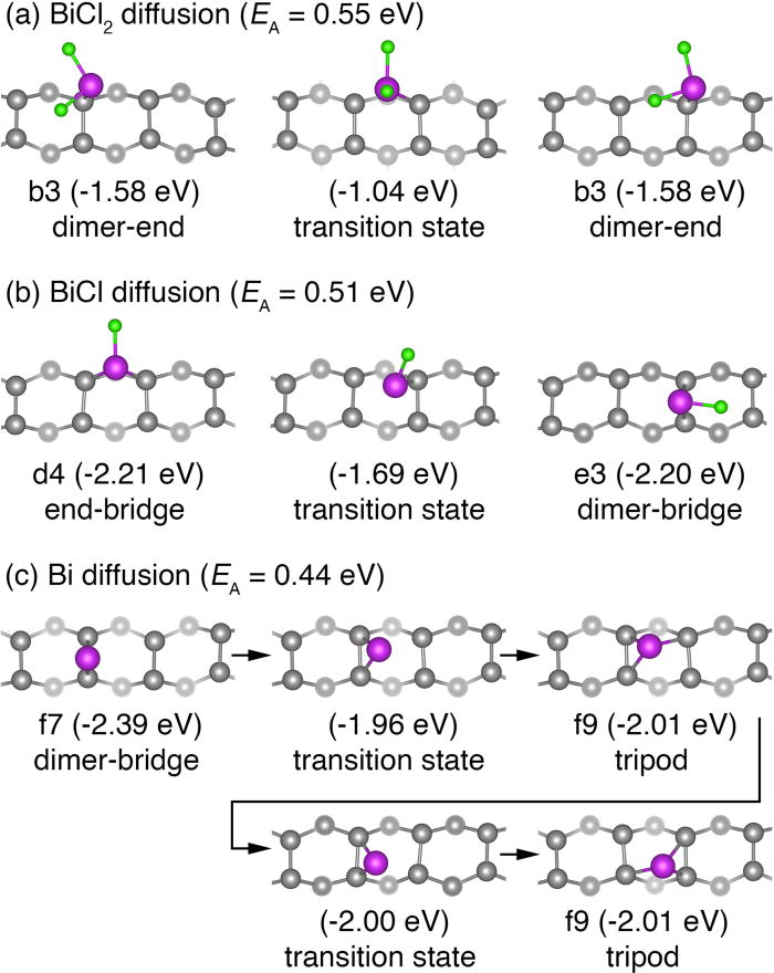
Bismuth trichloride as a molecular precursor for silicon doping
Applied Physics Letters
·
10 Apr 2023
·
doi:10.1063/5.0145772
Non‐Destructive X‐Ray Imaging of Patterned Delta‐Layer Devices in Silicon
Advanced Electronic Materials
·
25 Mar 2023
·
doi:10.1002/AELM.202201212
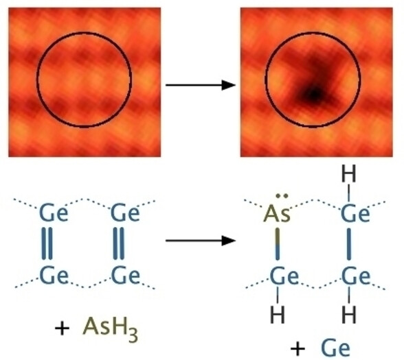
Room Temperature Incorporation of Arsenic Atoms into the Germanium (001) Surface**
Angewandte Chemie International Edition
·
10 Jan 2023
·
doi:10.1002/ANIE.202213982
This paper reports that arsenic incorporates into Ge(001) at room temperature, addressing a key challenge for scalable donor-based quantum devices.
2022
Atomic and molecular functionalisation of technological materials: an introduction to nanoscale processes on semiconductor surfaces
Journal of Physics: Condensed Matter
·
25 Mar 2022
·
doi:10.1088/1361-648X/AC5A24
2021
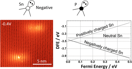
Substitutional Tin Acceptor States in Black Phosphorus
The Journal of Physical Chemistry C
·
11 Oct 2021
·
doi:10.1021/ACS.JPCC.1C07115
The formation of a Sn monolayer on Ge(1 0 0) studied at the atomic scale
Applied Surface Science
·
01 Sep 2021
·
doi:10.1016/J.APSUSC.2021.149961
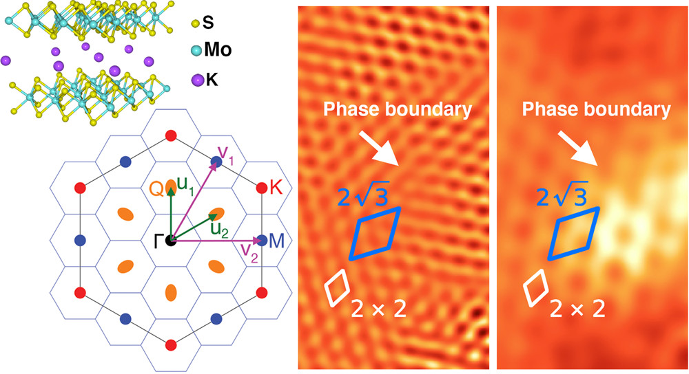
Charge Density Waves in Electron-Doped Molybdenum Disulfide
Nano Letters
·
06 Jul 2021
·
doi:10.1021/ACS.NANOLETT.1C00677
This paper reports the first observation of a charge density wave ground state in a semiconducting transition metal dichalcogenide, providing new insight into CDW formation mechanisms.
Determination of the preferred reaction pathway of acetophenone on Si(001) using photoelectron diffraction
Journal of Physics: Condensed Matter
·
04 May 2021
·
doi:10.1088/1361-648X/ABE6DD
2020
Atomic-Scale Patterning of Arsenic in Silicon by Scanning Tunneling Microscopy
ACS Nano
·
06 Mar 2020
·
doi:10.1021/ACSNANO.9B08943
2019
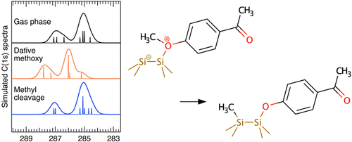
Dissociation of CH3–O as a Driving Force for Methoxyacetophenone Adsorption on Si(001)
The Journal of Physical Chemistry C
·
19 Aug 2019
·
doi:10.1021/ACS.JPCC.9B04954
2018
Two- to three-dimensional crossover in a dense electron liquid in silicon
Physical Review B
·
23 Apr 2018
·
doi:10.1103/PHYSREVB.97.155306
Higher order reconstructions of the Ge(001) surface induced by a Ba layer
Applied Surface Science
·
01 Mar 2018
·
doi:10.1016/J.APSUSC.2017.11.058
2017
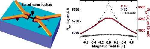
Nondestructive imaging of atomically thin nanostructures buried in silicon
Science Advances
·
02 Jun 2017
·
doi:10.1126/SCIADV.1602586
Exact location of dopants below the Si(001):H surface from scanning tunneling microscopy and density functional theory
Physical Review B
·
07 Feb 2017
·
doi:10.1103/PHYSREVB.95.075408
2016
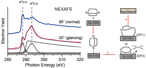
Adsorption and Dissociation of a Bicyclic Tertiary Diamine, Triethylenediamine, on a Si(100)-2 × 1 Surface
The Journal of Physical Chemistry C
·
07 Dec 2016
·
doi:10.1021/ACS.JPCC.6B10485
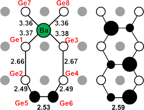
STM and DFT study on formation and characterization of Ba-incorporated phases on a Ge(001) surface
Physical Review B
·
09 May 2016
·
doi:10.1103/PHYSREVB.93.195304
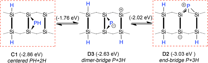
Reaction paths of phosphine dissociation on silicon (001)
The Journal of Chemical Physics
·
07 Jan 2016
·
doi:10.1063/1.4939124
Orientation and stability of a bi-functional aromatic organic molecular adsorbate on silicon
Physical Chemistry Chemical Physics
·
01 Jan 2016
·
doi:10.1039/C6CP04328C
2015
Initial growth of Ba on: An STM and DFT study
Physical Review B
·
29 Jun 2015
·
doi:10.1103/PHYSREVB.91.235319
Water-Induced, Spin-Dependent Defects on the Silicon (001) Surface
The Journal of Physical Chemistry C
·
13 May 2015
·
doi:10.1021/ACS.JPCC.5B01493
Ba termination of Ge(001) studied with STM
Nanotechnology
·
23 Mar 2015
·
doi:10.1088/0957-4484/26/15/155701
Single dopants in semiconductors
Journal of Physics: Condensed Matter
·
18 Mar 2015
·
doi:10.1088/0953-8984/27/15/150301
2014
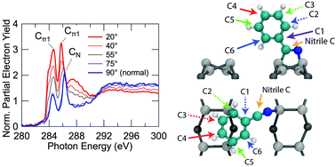
Manipulating the orientation of an organic adsorbate on silicon: a NEXAFS study of acetophenone on Si(0 0 1)
Journal of Physics: Condensed Matter
·
21 Nov 2014
·
doi:10.1088/0953-8984/27/5/054002
Organic molecules on inorganic surfaces
Journal of Physics: Condensed Matter
·
21 Nov 2014
·
doi:10.1088/0953-8984/27/5/050301
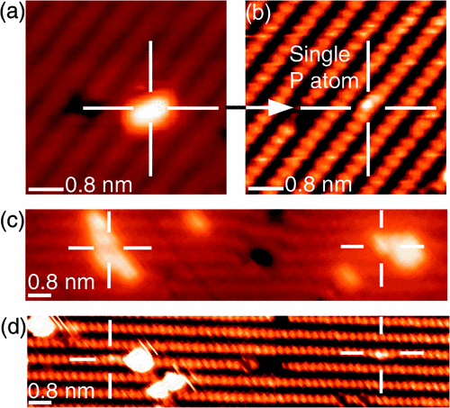
Imaging of buried phosphorus nanostructures in silicon using scanning tunneling microscopy
Applied Physics Letters
·
23 Jun 2014
·
doi:10.1063/1.4884654
Interface and nanostructure evolution of cobalt germanides on Ge(001)
Journal of Applied Physics
·
21 Feb 2014
·
doi:10.1063/1.4865955
2013

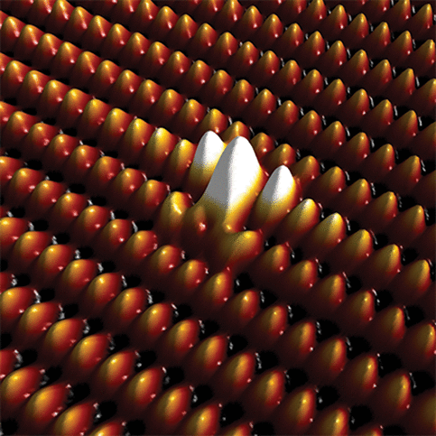
Investigating individual arsenic dopant atoms in silicon using low-temperature scanning tunnelling microscopy
Journal of Physics: Condensed Matter
·
04 Dec 2013
·
doi:10.1088/0953-8984/26/1/012001
Magnetic anisotropy of single Mn acceptors in GaAs in an external magnetic field
Physical Review B
·
12 Nov 2013
·
doi:10.1103/PHYSREVB.88.205203
Quantum engineering at the silicon surface using dangling bonds
Nature Communications
·
03 Apr 2013
·
doi:10.1038/NCOMMS2679
This paper reports the unanticipated discovery of a new atomic-scale quantum dot state in silicon, created by atomic manipulation on a hydrogen-terminated surface, providing key insights into atomic-scale quantum dot behaviour.
Phenyl Attachment to Si(001) via STM Manipulation of Acetophenone
The Journal of Physical Chemistry C
·
07 Mar 2013
·
doi:10.1021/JP311261R
Studying atomic scale structural and electronic properties of ion implanted silicon samples using cross-sectional scanning tunneling microscopy
Applied Physics Letters
·
07 Jan 2013
·
doi:10.1063/1.4772508
2012
Site-Dependent Ambipolar Charge States Induced by Group V Atoms in a Silicon Surface
ACS Nano
·
27 Nov 2012
·
doi:10.1021/NN3039484
Guided Self-Assembly of Metal Atoms on Silicon Using Organic-Molecule Templating
Journal of the American Chemical Society
·
05 Sep 2012
·
doi:10.1021/JA3026399
Slab Thickness Effects for the Clean and Adsorbed Ge(001) Surface with Comparison to Si(001)
The Journal of Physical Chemistry C
·
08 Mar 2012
·
doi:10.1021/JP208247M
2011
Charge density waves in the graphene sheets of the superconductor CaC6
Nature Communications
·
29 Nov 2011
·
doi:10.1038/NCOMMS1574
Acetic acid on silicon (001): An exercise in chemical analogy
Physical Review B
·
04 Oct 2011
·
doi:10.1103/PHYSREVB.84.153302
Model system for controlling strain in silicon at the atomic scale
Physical Review B
·
22 Jul 2011
·
doi:10.1103/PHYSREVB.84.041306
Dimer pinning and the assignment of semiconductor–adsorbate surface structures
The Journal of Chemical Physics
·
10 Feb 2011
·
doi:10.1063/1.3551618
2010
Electronic effects of single H atoms on Ge(001) revisited
The Journal of Chemical Physics
·
07 Jul 2010
·
doi:10.1063/1.3456736
Comment on “Transformation of C-type defects on surface at room temperature STM/STS study [Surf. Sci. 602 (2008) 2835]”
Surface Science
·
01 Jan 2010
·
doi:10.1016/J.SUSC.2009.10.028
2009
Radnyet al.Reply:
Physical Review Letters
·
30 Oct 2009
·
doi:10.1103/PHYSREVLETT.103.189702
Carbonyl mediated attachment to silicon: Acetaldehyde on Si(001)
The Journal of Chemical Physics
·
14 Sep 2009
·
doi:10.1063/1.3224174
Acetone on silicon (001): ambiphilic molecule meets ambiphilic surface
Physical Chemistry Chemical Physics
·
01 Jan 2009
·
doi:10.1039/B815542A
2008
Interaction of acetone with the Si(001) surface
Surface Science
·
01 Nov 2008
·
doi:10.1016/J.SUSC.2008.08.027
Electronic effects induced by single hydrogen atoms on the Ge(001) surface
The Journal of Chemical Physics
·
24 Jun 2008
·
doi:10.1063/1.2938091
Valence Surface Electronic States on Ge(001)
Physical Review Letters
·
20 Jun 2008
·
doi:10.1103/PHYSREVLETT.100.246807
Water on silicon (001):defects and initial steps of surface oxidation
Physical Review B
·
22 May 2008
·
doi:10.1103/PHYSREVB.77.201305
2007
Towards hybrid silicon-organic molecular electronics: The stability of acetone on the Si(001) surface
Surface Science
·
01 Dec 2007
·
doi:10.1016/J.SUSC.2007.06.054
Single P and As dopants in the Si(001) surface
The Journal of Chemical Physics
·
13 Nov 2007
·
doi:10.1063/1.2786991
Single hydrogen atoms on the Si(001) surface
Physical Review B
·
02 Oct 2007
·
doi:10.1103/PHYSREVB.76.155302
Organic Bonding to Silicon via a Carbonyl Group: New Insights from Atomic-Scale Images
Journal of the American Chemical Society
·
24 Aug 2007
·
doi:10.1021/JA0719069
2006
Thermal dissociation and desorption ofon Si(001): A reinterpretation of spectroscopic data
Physical Review B
·
08 Nov 2006
·
doi:10.1103/PHYSREVB.74.195310
Importance of charging in atomic resolution scanning tunneling microscopy: Study of a single phosphorus atom in asurface
Physical Review B
·
27 Sep 2006
·
doi:10.1103/PHYSREVB.74.113311
Phosphine Dissociation and Diffusion on Si(001) Observed at the Atomic Scale
The Journal of Physical Chemistry B
·
01 Feb 2006
·
doi:10.1021/JP054646V
Phosphorus and hydrogen atoms on the (001) surface of silicon: A comparative scanning tunnelling microscopy study of surface species with a single dangling bond
Surface Science
·
01 Jan 2006
·
doi:10.1016/J.SUSC.2005.10.031
Atomic-scale observation and control of the reaction of phosphine with silicon
e-Journal of Surface Science and Nanotechnology
·
01 Jan 2006
·
doi:10.1380/EJSSNT.2006.609
2005
Observation of substitutional and interstitial phosphorus on cleanwith scanning tunneling microscopy
Physical Review B
·
14 Nov 2005
·
doi:10.1103/PHYSREVB.72.195323
Phosphine adsorption and dissociation on the Si(001) surface: Anab initiosurvey of structures
Physical Review B
·
19 Sep 2005
·
doi:10.1103/PHYSREVB.72.125328
Scanning probe microscopy for silicon device fabrication
Molecular Simulation
·
01 May 2005
·
doi:10.1080/08927020500035580
2004
Phosphine Dissociation on the Si(001) Surface
Physical Review Letters
·
23 Nov 2004
·
doi:10.1103/PHYSREVLETT.93.226102
Toward Atomic-Scale Device Fabrication in Silicon Using Scanning Probe Microscopy
Nano Letters
·
28 Sep 2004
·
doi:10.1021/NL048808V
STM characterization of the Si-P heterodimer
Physical Review B
·
13 May 2004
·
doi:10.1103/PHYSREVB.69.195303
Split-off dimer defects on thesurface
Physical Review B
·
19 Feb 2004
·
doi:10.1103/PHYSREVB.69.085312
2003
Atomically Precise Placement of Single Dopants in Si
Physical Review Letters
·
25 Sep 2003
·
doi:10.1103/PHYSREVLETT.91.136104
This seminal paper presents the first demonstration of atomically precise dopant placement in a semiconductor, laying the foundation for modern atomic-scale quantum electronic devices.
Progress in silicon-based quantum computing
Philosophical Transactions of the Royal Society of London. Series A: Mathematical, Physical and Engineering Sciences
·
15 Jul 2003
·
doi:10.1098/RSTA.2003.1221
Scanning tunneling microscopy imaging of charged defects on clean Si(100)-(2×1)
Journal of Vacuum Science & Technology A: Vacuum, Surfaces, and Films
·
01 Jul 2003
·
doi:10.1116/1.1566973
Towards the atomic-scale fabrication of a silicon-based solid state quantum computer
Surface Science
·
01 Jun 2003
·
doi:10.1016/S0039-6028(03)00485-0
Critical issues in the formation of atomic arrays of phosphorus in silicon for the fabrication of a solid-state quantum computer
Surface Science
·
01 Jun 2003
·
doi:10.1016/S0039-6028(03)00206-1
Challenges in Surface Science for a P-in-Si Quantum Computer — Phosphine Adsorption/Incorporation and Epitaxial Si Encapsulation
Surface Review and Letters
·
01 Apr 2003
·
doi:10.1142/S0218625X03005098
2002
Encapsulation of phosphorus dopants in silicon for the fabrication of a quantum computer
Applied Physics Letters
·
21 Oct 2002
·
doi:10.1063/1.1516859
Scanning tunnelling microscope fabrication of arrays of phosphorus atom qubits for a silicon quantum computer
Smart Materials and Structures
·
20 Sep 2002
·
doi:10.1088/0964-1726/11/5/318
Imaging charged defects on clean Si(100)-(2×1) with scanning tunneling microscopy
Journal of Applied Physics
·
15 Jul 2002
·
doi:10.1063/1.1486047
2001
<title>Nanoscale phosphorous atom arrays created using STM for the fabricaton of a silicon-based quantum computer</title>
SPIE Proceedings
·
19 Nov 2001
·
doi:10.1117/12.454617
Towards the fabrication of phosphorus qubits for a silicon quantum computer
Physical Review B
·
21 Sep 2001
·
doi:10.1103/PHYSREVB.64.161401
2000
Energetics of single- and double-layer steps on thesurface calculated using the extended Brenner empirical potential
Physical Review B
·
15 Oct 2000
·
doi:10.1103/PHYSREVB.62.10199
The atomic fabrication of a silicon based quantum computer
Proceedings of the 2001 1st IEEE Conference on Nanotechnology. IEEE-NANO 2001 (Cat. No.01EX516)
·
[no date info]
·
doi:10.1109/NANO.2001.966469
Minimisation of P surface segregation during epitaxial silicon growth for the fabrication of a silicon-based quantum computer
2002 Conference on Optoelectronic and Microelectronic Materials and Devices. COMMAD 2002. Proceedings (Cat. No.02EX601)
·
[no date info]
·
doi:10.1109/COMMAD.2002.1237241