Two-dimensional (2D) materials
Two-dimensional materials provide a highly tunable platform for studying quantum states and defect physics at the atomic scale. Their reduced dimensionality, weak dielectric screening, and strong many-body interactions give rise to rich electronic behaviour that can be accessed and controlled with scanning tunnelling microscopy (STM).
We use ultrahigh-vacuum, low-temperature STM/STS to:
- identify and characterise intrinsic and extrinsic point defects in 2D materials
- map real-space electronic structure with atomic resolution
- quantify donor-, acceptor-, and mid-gap defect states
- engineer chemical substitution, doping, and charge environments
- investigate collective electronic phases such as charge density waves
These approaches allow us to understand and manipulate the electronic structure of 2D materials one atom at a time.
Atomic-scale defects and extended quantum states in 2D materials
Defects in 2D systems—whether substitutional impurities or vacancies—play an outsized role in determining local band structure, carrier density, and optical and transport properties. Our STM studies reveal their real-space structure and electronic signatures, providing insight relevant to quantum technologies and two-dimensional optoelectronic devices.
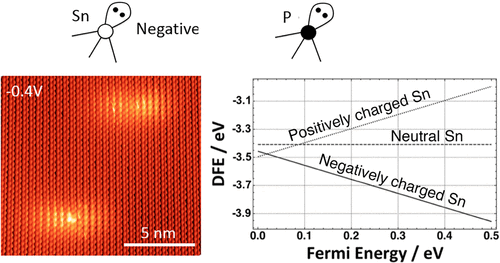
One long-standing question concerns the origin of p-type behaviour in nominally undoped black phosphorus. Using STM/STS combined with density functional theory calculations performed by Prof. Alex Shluger and his group, we showed that ultra-low concentrations of substitutional tin impurities are present in typical samples. These impurities are difficult to detect using conventional methods but are readily identifiable in STM.
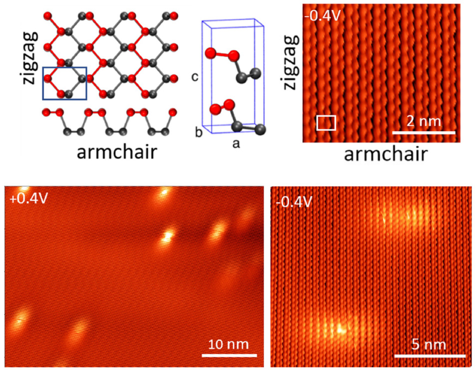
Figure 1: STM image of atomic-point defects in black phosphorus, identified as substitutional Sn impurities.
The extended, anisotropic acceptor-like wave function is characteristic of the shallow hydrogenic
bound state (J. Phys. Chem. C 2021, 125, 41, 22883–22889).
Each Sn impurity produces a spatially extended, anisotropic acceptor-like hydrogenic state, visible as a characteristic lobed feature in STM topographs. The defect arises from a tin atom substituting at a phosphorus site, introducing a local perturbation to the electronic structure that binds a hole.
This work established a clear connection between atomic structure and defect-induced electronic properties in black phosphorus, resolving several earlier ambiguities regarding its intrinsic defect landscape.
Charge density waves in 2D materials
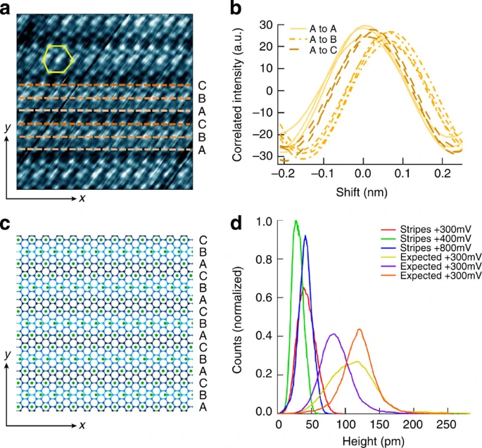
Transition-metal dichalcogenides (TMDs) exhibit strong electron correlations and can host emergent phases under doping. By intercalating charged ions into the vdW gaps, in collaboration with Prof. Chris Howard’s group at UCL, and measuring with STM/STS, we obtained the first atomic-scale evidence for a charge density wave (CDW) in heavily electron-doped MoS₂ and CaC₆.
Excess charge, introduced via interstitial dopants, drives the formation of an ordered modulation of the electronic density. STM images show a clear periodic modulation superimposed on the surface atoms lattice, and spectroscopy reveals a partial gap opening consistent with CDW formation.
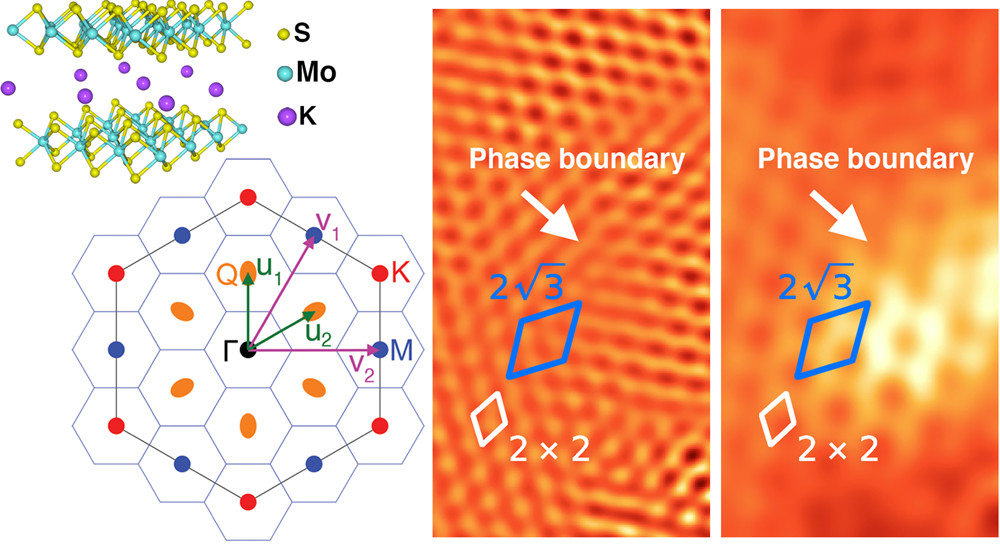
Figure 2: Heavily electron-doped MoS₂ formed by potassium intercalation into the vdW gaps. Two separate CDW modulations are observed in cryogenic-temperature STM (Nano Lett. 2021, 21, 5516–5521).
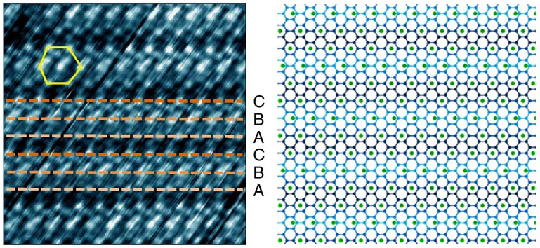
Figure 3: STM image of CDW modulation in CaC₆. (Nature Communications 2, 558 (2011)).
These studies highlight how controlled doping—whether intentional or defect-driven—can induce correlated phases in 2D semiconductors. They also demonstrate the ability of STM to directly visualise these emerging electronic orders. Unique to STM, we are also able to explore the role of individual defect states to the formation of these ordered phases, which was particularly relevant in the case of MoS₂ where two different modulations were found, one of them occuring only at defect sites.
Selected publications