Quantum state imaging
Quantum state imaging is one of the core research activities of our group. We use low-temperature scanning tunnelling microscopy (STM) and spectroscopy to visualise the extended quantum states of dopants and defects in semiconductors, revealing their symmetry, spatial extent, and interactions with the surrounding lattice.
Our work combines:
- Ultrahigh vacuum (UHV) cryogenic STM (atomic-resolution imaging and spectroscopy)
- Semiconductors and two-dimensional (2D) materials
- Donors, acceptors, deep centre defects
- Tight-binding, effective-mass theory, and density functional theory (via collaboration)
Together, these approaches allow us to probe and understand the real-space wave functions of individual impurities and engineered atomic-scale structures.
Imaging a wide range of quantum states
We explore a broad range of defects in semiconductors and two-dimensional materials that support remarkably varied quantum states. These span shallow hydrogenic dopants, deep-level defects, vacancy-derived states, and extended structures engineered directly on semiconductor surfaces.
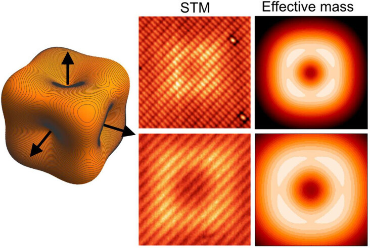
A major milestone from our group was the first real-space imaging of the hydrogenic acceptor wave function in silicon. This was achieved by implanting high-energy bismuth ions to create acceptor defects below the surface. The resulting quantum states exhibit a distinctive square-ring appearance in STM images—an anisotropic envelope that is accurately reproduced by both effective-mass and tight-binding calculations.
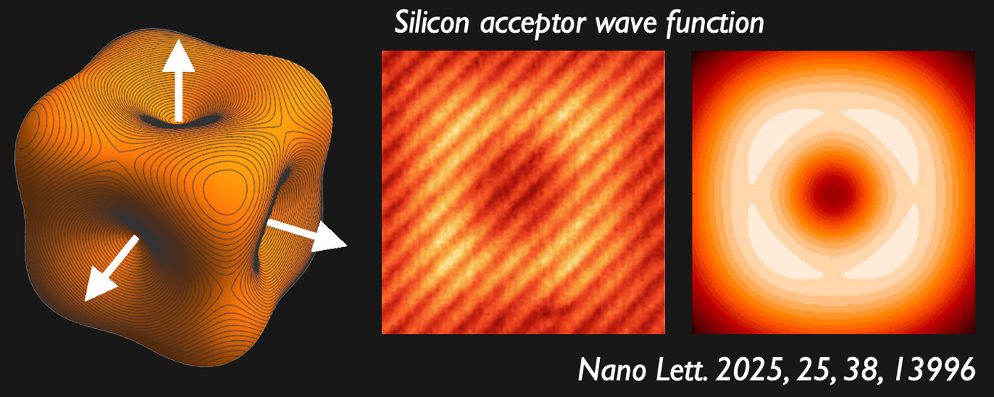
Figure 1: STM image and effective-mass calculation of a single acceptor state in silicon.
The STM image (middle) shows the anisotropic wavefunction amplitudes of the buried acceptor
state on H–Si(001). The effective-mass calculation is shown in 3D and as a simulated STM
contrast (Nano Lett. 2025, 25, 38, 13996–14001).
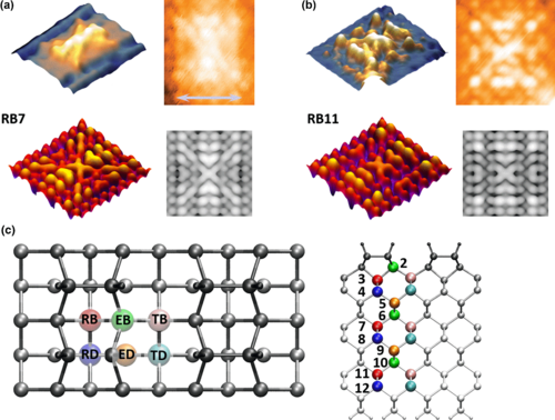
Beyond dopants, we have also uncovered excited-state behaviour in dangling bonds (DBs) on the hydrogen-terminated Si(001) surface. A single DB acts as a deep-centre defect—similar to the Pb-centre—with a ground and an excited state that can be resolved directly in STM.
By engineering closely spaced pairs and larger DB assemblies, we demonstrated that these excited states hybridise across the structure. The signature is unmistakable: a maximum of intensity appears between DBs, exactly where a simple ground-state-only picture would predict a minimum. This provides clear experimental evidence for the formation of molecule-like excited states in surface-engineered quantum structures.
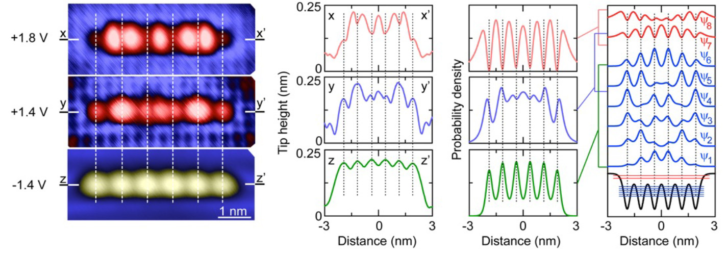
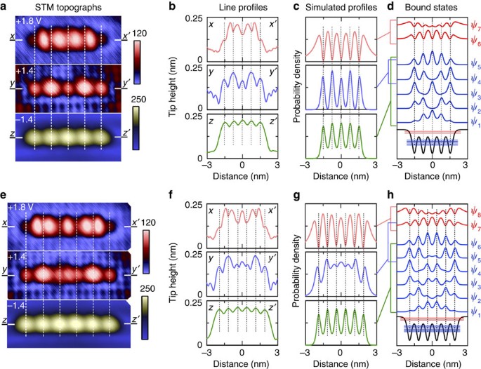
Figure 2: Atomic-scale quantum dot fabricated from dangling bonds on a hydrogen-terminated
Si(001) surface. The six-dot system was formed by removing hydrogen atoms individually, and
supports hybridised ground and excited states extending across the full structure
(Nature Communications 4, 1649 (2013)).
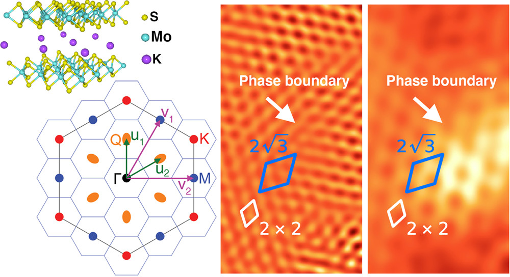
We have also investigated a wide range of other quantum systems, from defect-induced charge density waves in electron-doped MoS₂ to the hydrogenic donor wave function of arsenic in silicon. Details of these studies can be found in the selected publications listed below.
Selected publications