Measuring the thickness of δ-doped layers with SX-ARPES
We can create atomically thin δ-doping planes in silicon and germanium that are highly conducting and useful for building atomic-scale electronic and quantum devices. However, measuring the true thickness of these layers is difficult. Techniques such as secondary ion mass spectrometry (SIMS) do not have the spatial resolution needed to distinguish layers just a few atomic planes thick.
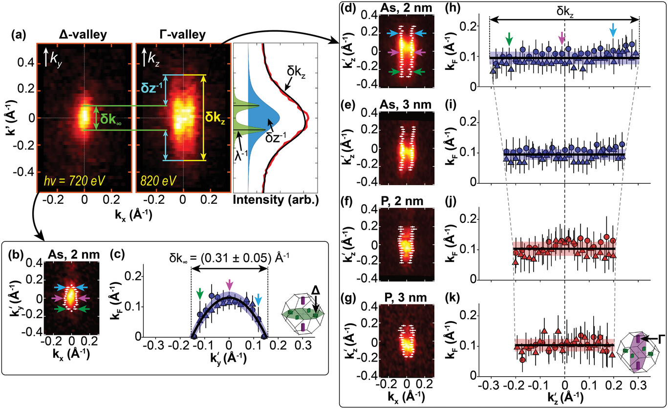
To address this challenge, we use soft X-ray ARPES (SX-ARPES). The relatively high photon energies (300–800 eV) allow us to probe electronic states located several nanometres beneath the surface while still resolving their momentum structure across multiple Brillouin zones.
By analysing the energy and momentum of electrons confined in the two-dimensional potential formed by the dopant layer, we find that the electronic thickness of these δ-layers is only about 5 Å, or roughly three silicon crystal planes. This is possible because the photoemission intensity is related to the real-space wave function through a Fourier transform, which allows SX-ARPES to reveal how tightly the electrons are confined.
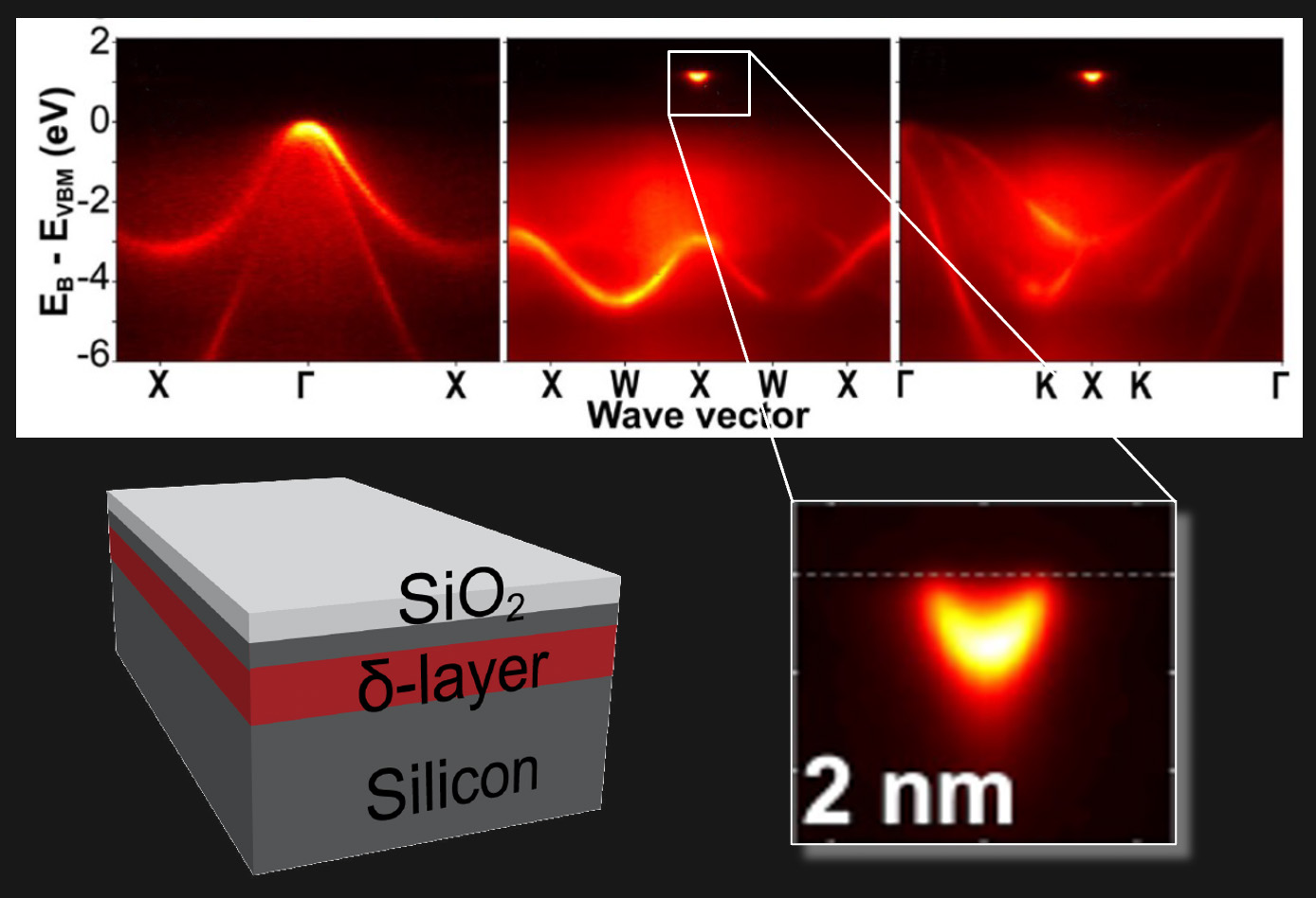
Figure: SX-ARPES measurement from a silicon crystal containing a δ-doped layer 2 nm beneath the surface. The two-dimensionally confined δ-band pocket can be seen near the conduction-band minimum at the X-point, revealing the quantum well formed by the dopant atoms.
More detail can be found in our publications.
Selected publications