Research overview
Our group studies the quantum properties of matter at the atomic scale, with a focus on scanning tunnelling microscopy (STM), angle-resolved photoemission spectroscopy (ARPES), and the theory of defects and dopants in semiconductors and 2D materials.
This page presnts short summaries of our main research themes together with selected talks and presentations.
Selected Research Topics

Imaging the quantum states of single dopants and defects with atomic-resolution STM to uncover their symmetry, spatial extent, and electronic behaviour.

We probe the electronic structure of quantum systems buried inside silicon by using soft X-ray ARPES to access their full three-dimensional band structure.
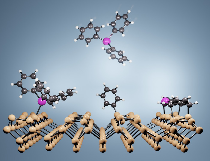
We investigate how individual molecules adsorb, bond, and react on semiconductor surfaces using atomic-resolution STM combined with first-principles DFT modelling. This work underpins the development of atomically precise dopant incorporation in semiconductors and lays the foundation for atomic-scale electronic devices.
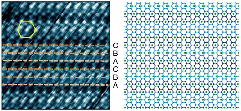
We use low-temperature STM/STS to identify and manipulate atomic-scale defects in two-dimensional materials. Our work spans the imaging of substitutional impurities, mapping of hydrogenic defect states, and the discovery of emergent phases such as charge density waves in heavily electron-doped MoS₂.
Research Presentations
A tour of atomic-scale fabrication with STM, real-space imaging of dopant and defect quantum states, and soft X-ray ARPES studies of buried interfaces and δ-doped layers.