Plenary Lecture at GADEST 2026, Venice
 Steven Schofield
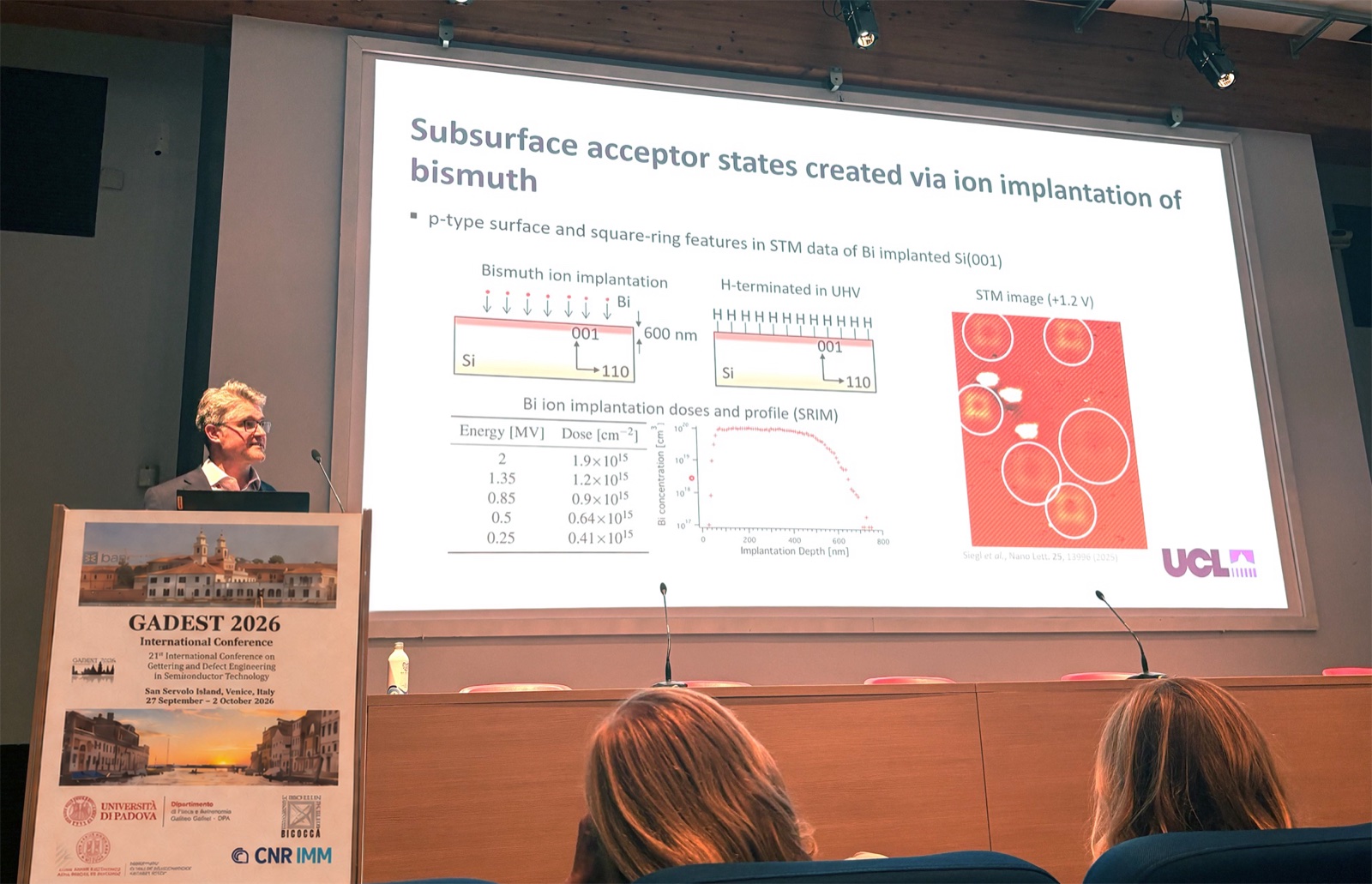
Last week I delivered the plenary lecture at GADEST 2026, the 21st International Conference on Gettering and Defect Engineering in Semiconductor Technology, held on San Servolo Island in the Venice lagoon.
GADEST dates back to 1985, when the first meeting was held in Garzau in what was then the German Democratic Republic. Since then, the biennial series has expanded to venues across Europe, including Belgium, France, Sweden, the UK (Oxford), Austria, Georgia, and Italy. This was my first time attending, but I doubt it will be my last. There were over 130 participants from 21 countries, with talks ranging from the mechanisms of gettering and defect formation to device processing and modelling, photovoltaics, and quantum information technology. Several talks touched on qubits, including my own on dopant qubits in silicon and germanium and others on quantum dot qubits. There was plenty of interest for our group, and I anticipate our group participating in future GADEST meetings.
My talk, Dopants at the Atomic Limit in Silicon and Germanium, gave an overview of our group’s work on atomic-scale dopant systems. We combine ultrahigh vacuum scanning tunnelling microscopy, soft X-ray angle-resolved photoemission spectroscopy, and theoretical modelling to understand how dopant species, host material, and fabrication methods affect incorporation, electronic structure, and quantum confinement. I covered work on alternative dopant chemistries and ultra-confined doped layers, as well as the anisotropic dopant wavefunctions we have imaged directly in silicon.
Some of the most useful conversations over coffee concerned quite specific questions. One discussion about whether bismuth diffuses in silicon, and the structural defects it can form, was particularly relevant to a question we are working on in the group at the moment. I also discovered a supplier for one-off academic semiconductor wafers that my group was not aware of, which may prove useful for future experiments. It was also a good chance to make new contacts closer to home: several UK academics working on photovoltaics, a field I don’t work in directly, but very much part of the same semiconductor community, and it was great to finally meet them in person. Alongside the talks, these were good reasons to have made the trip.
This was also my first time in Venice. It is difficult to write about without reaching for cliché, because so much of it really does match the picture you have in your head from childhood. The canals, the gondolas, the picturesque buildings filled with artwork, the restaurants serving beautiful food, and more gelaterias than I have ever seen in one place: all of it lived up to expectations. What I had not anticipated was everything surrounding that image: that you can travel direct from the airport to the city entirely by boat, winding through the lagoon, which turned out to be a genuinely enjoyable way to arrive; the constant traffic of boats criss-crossing the water; and the sheer scale of the lagoon itself, scattered with islands each with their own character. One thing I missed out on was a swim. I learned too late that some of the other attendees had taken a boat across to Lido island, where you can swim facing out to the open sea. I’ll be sure to go there when I return to Venice with my family.
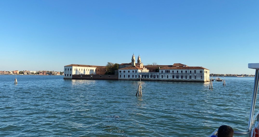
San Servolo island itself has a long and varied history, including a period as a psychiatric hospital, and is now an excellent conference venue. It felt remarkably peaceful: the island’s walls run straight to the water’s edge, with grassed and tree-lined courtyards inside. There is a restaurant and cafe on the island too, and you can stay there simply as a tourist, which I would happily do another time. It was a lovely place to spend the week, with plenty of space to sit and talk between sessions.
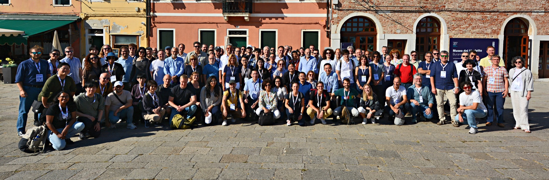
The conference programme included a social excursion to Burano, the small lagoon island famous for its brightly coloured houses and centuries-old tradition of lace-making. It felt quite different from Venice proper, with houses painted in vivid colours and a church tower leaning noticeably off vertical, which, on the soft, silty ground the whole lagoon is built on, seems to be more the rule than the exception. We gathered for the photograph below shortly after a delicious seafood lunch, with the Burano lace museum in the background.
Many thanks to the organisers, Enrico, Michele, Daniela, Simona, and Antonino, for putting together such a well-run and enjoyable meeting, and for the invitation to give the plenary lecture. I left already looking forward to the next edition of this engaging and interesting conference series that explores one of my favourite topics - the nature of defects in semiconductors!