Steven R. Schofield Research Group University College London (UCL)

Presentations

Selected research seminars and public lectures from the group.

Video Presentations
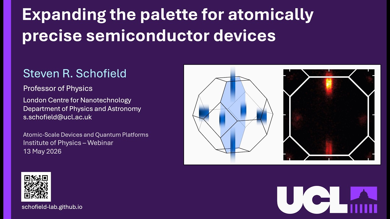
Expanding the Palette for Atomically Precise Semiconductor Devices
Expanding the Palette for Atomically Precise Semiconductor Devices Steven R. Schofield (Invited), 13 May 2026, IOP Webinar — Atomic-Scale Devices and Quantum Platforms

An short invited talk covering recent advances in atomically precise semiconductor device fabrication and quantum state imaging, delivered as part of the IOP Webinar series on Atomic-Scale Devices and Quantum Platforms.
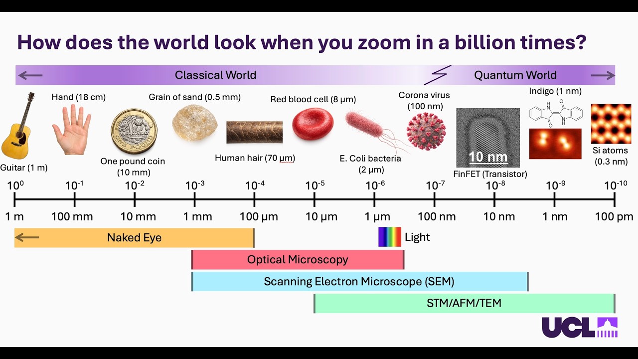
Seeing the Quantum World Electrons, Atoms, and Tunnelling Microscopy
Seeing the Quantum World — Electrons, Atoms, and Tunnelling Microscopy Steven R. Schofield, 21 May 2026, Public Lecture for Visiting High School Students, University College London

A public lecture covering wave–particle duality, the double-slit experiment with electrons, quantum tunnelling, and scanning tunnelling microscopy, finishing with the vision of using quantum states in semiconductors as the building blocks of a quantum computer.

Presentations — Slides Only
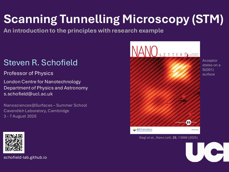
Scanning Tunnelling Microscopy STM
Scanning Tunnelling Microscopy (STM) Steven R. Schofield, 3–7 August 2026, Nanosciences@Surfaces Summer School, Cavendish Laboratory, University of Cambridge

An introduction to the principles of scanning tunnelling microscopy with a research example, delivered as a teaching lecture at the IOP Thin Films & Surfaces Group / CORDE Nanosciences@Surfaces Summer School.
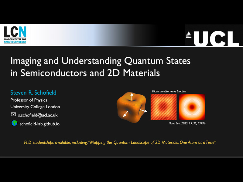
Imaging and Understanding Quantum States in Semiconductors and 2D Materials
Imaging and Understanding Quantum States in Semiconductors and 2D Materials Steven R. Schofield (Invited), 17 November 2025, Quantum Meets Nano Workshop, Institute of Physics, London, UK

A tour of atomic-scale fabrication with STM, real-space imaging of dopant and defect quantum states, and soft X-ray ARPES studies of buried interfaces and δ-doped layers.

Poster Presentations
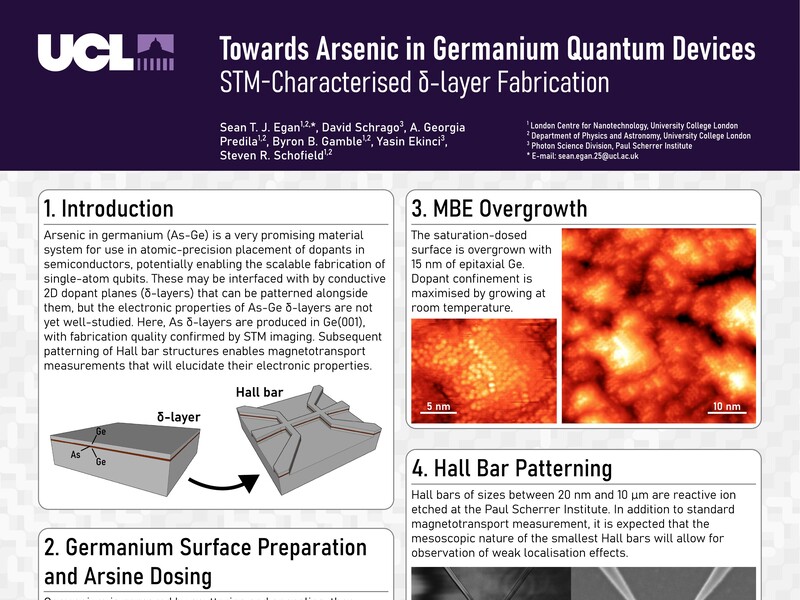
Towards Arsenic in Germanium Quantum Devices
Towards Arsenic in Germanium Quantum Devices Sean T. J. Egan (Presenting), David Schrago, A. Georgia Predila, Byron B. Gamble, Yasin Ekinci, Steven R. Schofield, 3–7 August 2026, Nanosciences@Surfaces Summer School, Cavendish Laboratory, University of Cambridge

STM-characterised δ-layer fabrication of arsenic in germanium, from surface preparation and arsine dosing through MBE overgrowth and Hall bar patterning, en route to scalable atomic-precision quantum devices.