Nanoscience@Surfaces Summer School 2026
 Sean Egan
Last week, I had the opportunity to attend the Nanoscience@Surfaces Summer School 2026 in Cambridge.
The school was held at the newly-relocated Cavendish Lab, in the Ray Dolby Centre - an absolutely stunning building, and furthermore an incredibly spacious one (which it’s difficult not to be a little envious of, coming from a central London institution!). The whole event was organised by Jack Kelsall, whom I knew beforehand as one of our collaborators in the surfaces group at Cambridge, and Viv Thomas, from the IoP. Putting together all the moving parts of a conference seemed like an incredibly tricky task from my perspective, but they managed it very well. Thank you, Jack and Viv!
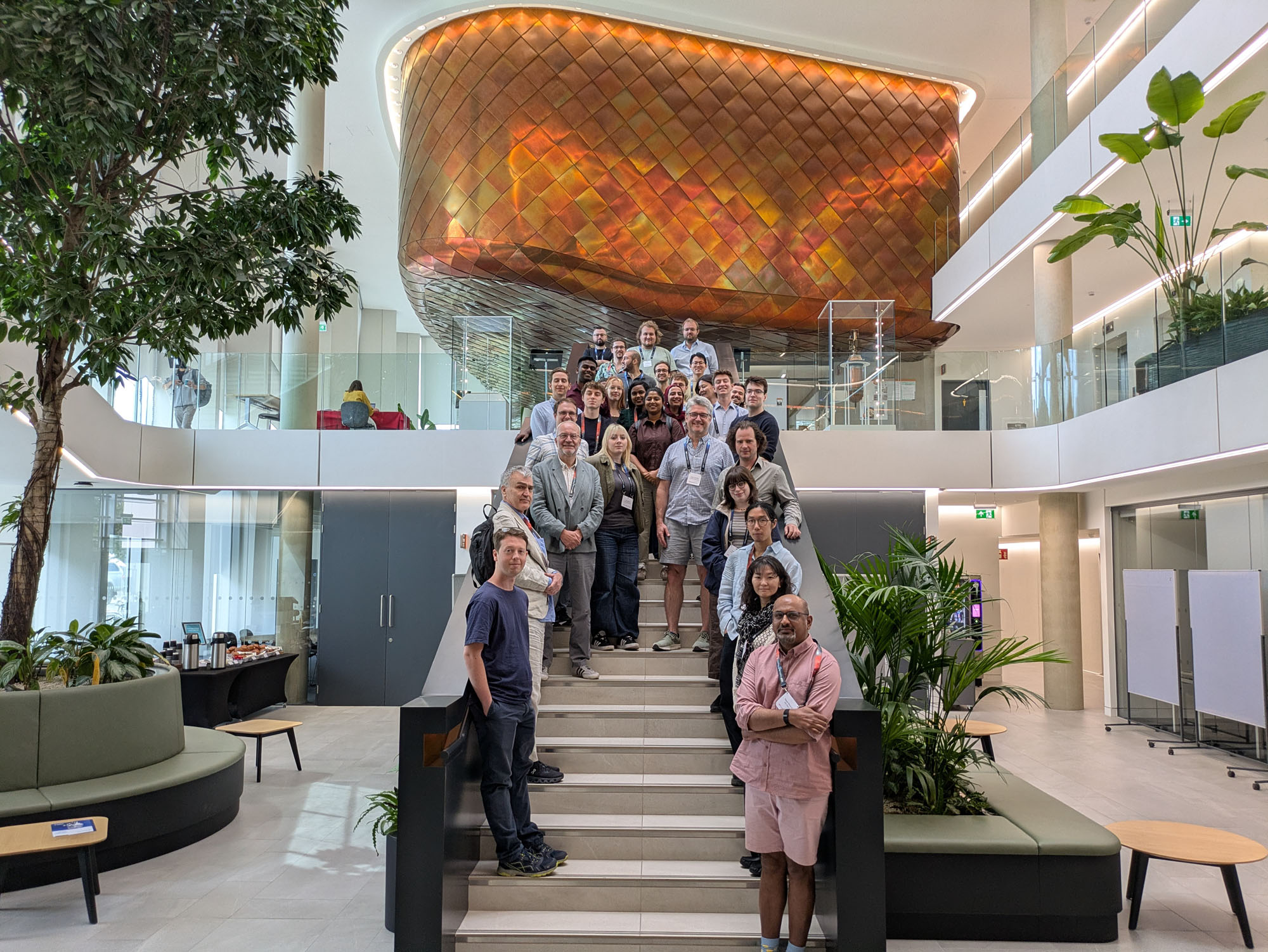
The talks and workshops given throughout the week provided interesting insight into many experimental techniques used for the characterisation of surfaces - from the familiar to the alien. There were many great talks given, to the point that it’s difficult to single out specific highlights, but one I found interesting was Shaoliang Guan’s talk and workshop on XPS - especially the use of near-atmospheric-pressure techniques. As someone planning to perform XPS experiments myself at the PSI next year, I was amazed by implementation in an atmosphere over ten orders of magnitude higher than normal. In NAP-XPS, UHV is maintained in the electron analyser using differential pumping whilst the sample is exposed to a gas, which allows for characterisation of reactions on surfaces as they occur. For me, though, the interest is mostly academic - I have more than enough UHV science to get through on silicon and germanium, at least for the time being.
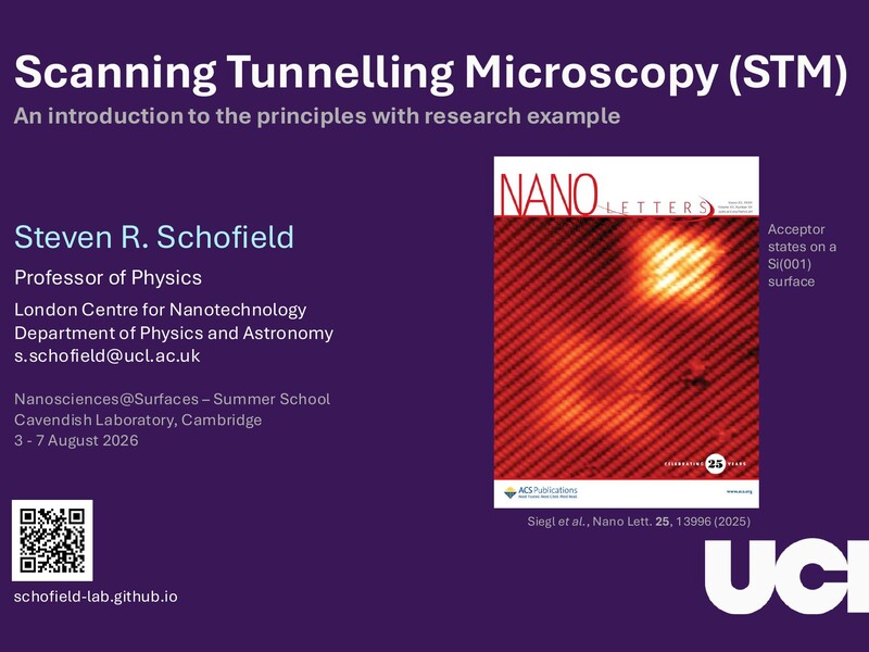
The STM and SEM workshops on Thursday were another highlight. In the STM workshop, I got to “impress” my fellow attendees by making PtIr tips - then dropping them while trying to transfer them into the miniscule benchtop system. I blame the tweezers. In seriousness, though, working with undergraduate-level equipment puts into perspective just how complex UHV STM is - and how effective and reliable. While I eventually got an image out of the pyrolitic graphite sample we were given, I was missing our system the entire time I was doing it.
The SEM workshop, meanwhile, was interesting to me on account of the SEM’s role in the work of our collaborators at the PSI, where it is currently being used to support the nanofabrication of Hall bar structures on the delta-layer samples I grew over the past couple of months. As well as imaging (lightning-fast compared to STM), I got to see the use of a focused ion beam to perform micro-milling of the surface, a technique that may be used to provide cross-sections for TEM imaging, but may also be used for etching, paralleling STM lithography in its serial nature. Another interesting technique that was demonstrated was electron beam-induced deposition of metallic structures. I’m intrigued by how these nanofabrication methods might complement our STM and EUV lithography, and hopefully, what I’ve learned will be helpful when I next visit the PSI.
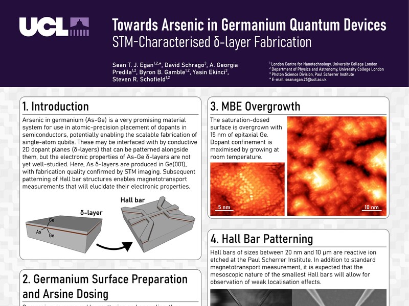
No discussion of the conference would be complete without me mentioning my poster. It was hard work producing it in time for the conference, with the time between the start of data collection and printing being about five weeks, but I’m very pleased with how it came out - some have described it as the best-looking poster of the lot! This early in my work, it’s hard to produce a poster with a lot of scientific content, so no prize this year, but I’m very pleased with the foundation I’ve laid for next time.
A PDF version of my poster is available on the presentations page of this website. My supervisor also attended for a day and gave the STM talk at the conference, and his slides are available there too.